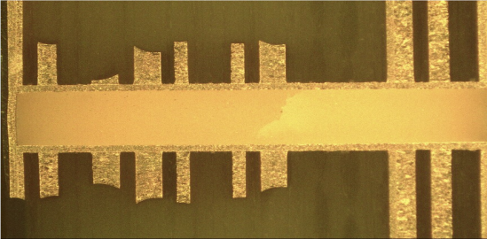
After 2 months of R&D and production, we Eagle Driver has once again completed this high-end, multilayer(10 layers) thick copper & blind vias & cu-inlay PCB board.
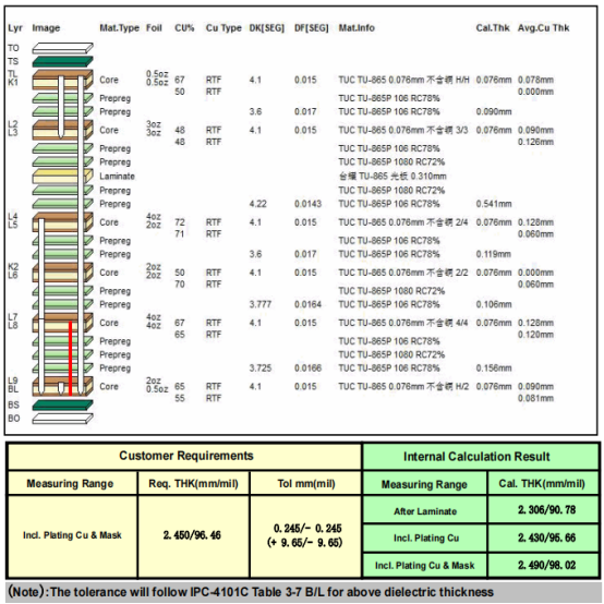
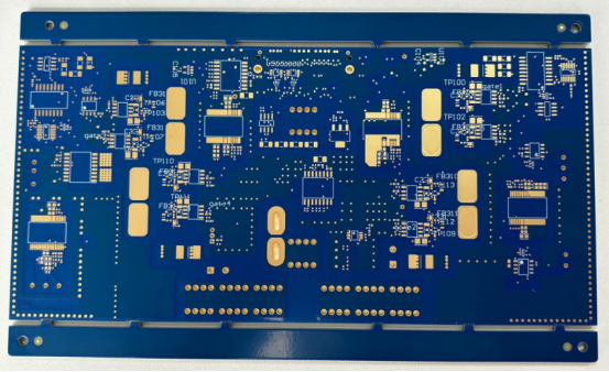
The specifications of this board are as follows: 10 layers of blind holes, board material: TU-865, TG200 ℃. Board thickness: 2.45mm. blind hole structure: L1-L3; L4-L10; L7-L10; L9-L10. The inner and outer copper thickness is 2/3/4/4/2/2/4/4/3/2 OZ. The plated slots need to be embedded with copper blocks, the slot size is 6*10mm, 8 slots per board.
The stack-up is as below:
The difficulty of this board is:
1. The blind hole board has a complex structure and needs to go through 4 lamination processes. The stack-up is asymmetrical and the copper is thick in both inner and outer layers. Our Eagle driver R&D engineers followed up on the whole process of lamination. Finally, the customer's copper thickness and dielectric thickness requirements were perfectly met.
2. The plated slots need to be embedded with copper blocks. The slots are large in size and there are 8 of them on each board. The electrical performance and heat dissipation functions of the specific layer need to be met. In addition, the customer has strict flatness requirements.
So, what is the buried/embedded copper block process?
buried/embedded copper block, The PCB industry is also called cu-inlay.
It is to precisely embed metal copper blocks inside the PCB to improve the heat dissipation performance significantly. We use advanced technology to closely combine the copper block with the PCB substrate to form an efficient heat dissipation channel. This process not only utilizes the high thermal conductivity of copper but also achieves rapid conduction and dissipation of heat through precise layout.
The PCB carrying the copper block can be designed as a multi-layer board, and the substrate material can be selected from FR4 (epoxy resin) material or high-frequency mixed material according to the product structure design needs.
Why does the PCB board need to introduce a cu-inlay process?
As electronic products become smaller and smaller, the size of printed circuit boards (PCB) is also shrinking, and circuit design is becoming more and more intensive. As the power density of components increases, the heat dissipation of PCBs is too large, which affects the service life, ageing and even failure of components. In addition, some crisis phenomena such as mobile phone battery explosions and car spontaneous combustion in recent years have always alerted people to the urgency of thermal management of electronic products. Based on the development of new generation information technology, energy-saving and new energy vehicles, power equipment and other fields, the solution to the heat dissipation problem is imminent.
There are many ways to solve the heat dissipation problem of PCB, such as dense heat dissipation hole design, thick copper foil circuit, metal base (core) board structure, embedded copper block design, copper base boss design, high thermal conductivity materials, etc. Directly embedding metal copper blocks in PCB is one of the effective ways to solve the heat dissipation problem.cu-inlay design is mainly divided into two categories: one is the semi-buried copper block type, named "buried copper block"; the other is the through-type, named "embedded copper block".
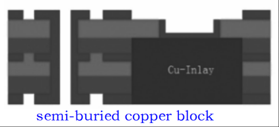
Buried copper block: The thickness of the buried copper block is less than the total thickness of the board. One side of the copper block is flush with one of the outer or inner layers, and the other side is flush with the other layers of the inner layer, as shown in Figure 1(semi-buried copper block).
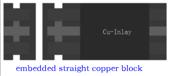
Embedded copper block: The thickness of the embedded copper block is close to or equal to the total thickness of the board, and the copper block runs through the entire board thickness. This type of copper block design includes embedded straight copper blocks and embedded step copper blocks.
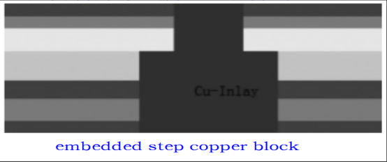
The main technical difficulties of cu-inlay are:
1. Matching of the copper block dimension and the milling size of the board: The copper block is placed in the milling area. If the copper block is too loose or too tight, it will affect the quality of the lamination filling process and bonding strength.
2. Flatness control of the copper block and board: During lamination, the flatness of the copper block and FR-4(or other material) core board is difficult to control. It is necessary to ensure that the flatness of the copper block and board is controlled within ±0.075 mm.
3. The residual glue on the copper block is difficult to remove: the resin overflowing from the gap between the copper block and the board during the lamination process and flowing to the residual glue on the copper block is very hard to remove, which will affect the reliability of the product.
4. Reliability of copper block and board: There is a certain height difference between the copper block and the FR-4(or other material) core board during the lamination process, which can easily lead to problems such as insufficient glue filling, voids, cracks, delamination, etc. at the connection between the copper block and the board.
The cu-inlay process of the multilayer board is as follows:
Cutting (copper block, FR4 substrate/high-frequency substrate, etc., prepreg) → inner layer circuit → inner layer AOI → OPE punching → inner core and prepreg milling → browning → riveting → lamination(placing copper block) → remove excess glue(grinding board) → controlled depth milling → mechanical drilling (including drilling blind holes) → copper plating → board electricity → outer layer circuit → graphic plating → outer layer etching → outer layer AOI → solder mask → silkscreen → chemical nickel/gold plating → outline→ electrical testing → finished product inspection.
Key manufacturing technologies and control measures:
1. Copper block forming
There are three main methods for copper block forming: the first method is to directly mill out the copper block of the required size through a special milling machine, but it needs to be equipped with a metal substrate milling machine and a special milling cutter, which is costly;
The second method is to use a milling machine for secondary processing, a milling machine with a controlled depth milling function, and a drill-tipped double-edged milling cutter for rough milling first and then fine milling, but it needs to be equipped with a milling machine with a controlled depth milling function and a special costly milling cutter.
The third method is to use a punch press for punching, which has high production efficiency, but the mould cost is high, the production flexibility is poor, and it is not suitable for sample or small batch production. In order to solve the above problems, a graphic etching and milling machine processing technology has been developed. First, the copper block graphic is transferred, and then the copper block shape is etched out by an etching machine, and then the copper block shape is processed for secondary processing with a conventional milling cutter and milling machine, so the production efficiency is high and the production cost is relatively low.
2. Milling slots on core and prepreg
According to the laminated structure, at first milling out the core and prepreg, and then riveted together, which has high-quality reliability.
3. Copper block lamination
Before laminating the copper block, the copper block must be horizontally browned and browning auxiliary tools (such as mesh drag swab) must be used to prevent the copper block from being too small, causing the machine to jam or fall into the cylinder, to ensure the micro-etching effect of the copper block. To improve the flatness and reliability of the copper block and the board(or mixed area), except to consider the matching between the copper block thickness and the board thickness, it is also necessary to select suitable buffer materials such as release film, aluminium sheet, and buffer pad. The laminated structure design is further optimized, and the high resin content prepregs and a special laminate process for the cu-inlay area fill the resin and completely cure the material to ensure heat resistance and insulation of the product.
After the product was manufactured, we conducted a series of tests, such as the flatness test of the embedded copper block and the board surface.
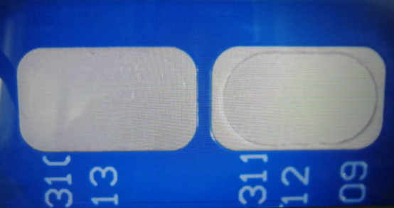
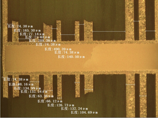
Thermal stress test, refer to IPC-TM-650, 2.6.8 Thermal stress test of plated holes; IPC-6012C Qualification and performance specifications for rigid printed boards. (Baking conditions: 121 ℃ ~ 149 ℃, at least 6 h; thermal stress test conditions: 288 ± 5 ℃, 10 s, 3 times).
The test results are: after the samples were tested according to the above test method, there were no voids, cracks, delamination, etc. in the gap between the copper block and the board, and the heat resistance was good.
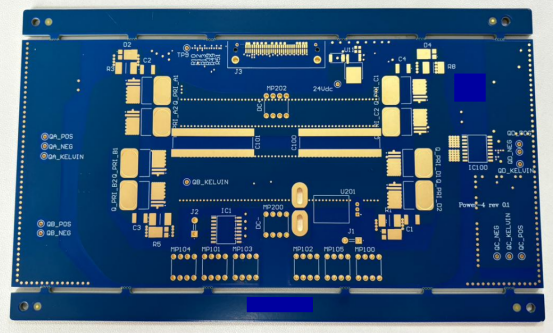
The actual PCB pictures as below:
The heat dissipation of the microwave PCB has always been one of the issues that the electronics industry pays more attention to. How to reduce the dielectric thickness of the RF(radio frequency) layer, reduce the surface roughness of the copper foil, and shorten the heat dissipation path and heat generation? The main way is to improve the thermal conductivity of the microwave substrate, dense heat dissipation holes or local thick copper plating or microwave layer thick copperization, and local embedded heat dissipation copper blocks. It can be foreseen that in the subsequent development of PCBs, the cu-inlay technology design will be the preferred solution.
Now, our Eagle Driver has reached the top level in China in terms of cu-inlay technology. After many rounds of research and development and trial production, we are now capable of mass production. On the premise of meeting the electrical performance and heat dissipation functions of a specific layer, the flatness, reliability and bonding strength of the buried/embedded copper block can also meet the industry's extremely high standards.
